
When I left off in the previous post, I had a working oscillator, but there were still some unresolved issues. We had a functioning oscillator, yet:
- The resonance point was incorrect and could not be calibrated.
- The startup time was unreasonably long.
The second version of this circuit will attempt to address both issues by changing the amplifier topology.
Eliminating Miller Effect Capacitance
In the first single-transistor version of the circuit, it could not be calibrated to the correct frequency; it would oscillate too low or not at all, strongly suggesting that we had too much loading capacitance. A few options immediately come to mind that can present a lower input capacitance:
Cascode
The cascode configuration lowers the effective input capacitance by mitigating the Miller effect, keeping the collector of the input transistor at a near-constant voltage. However, it comes at the cost of reduced output voltage swing, meaning I would need a higher supply voltage. All the same, it may be worth exploring this option.
Common Base
The common-base configuration is also effective at reducing input capacitance and has the additional benefit of allowing the base junction to act as a grounded shield, further reducing any capacitive coupling between the input and output. These attributes make it a staple topology in RF applications. Its steep downside, however, is that it provides no current gain. Since our crystal resonator already deals with tiny currents, this topology doesn’t immediately strike me as the best solution.
Long Tailed Pair
Although typically used as the backbone of differential amplifiers such as op-amps, the long-tailed pair is a flexible topology that presents low input capacitance, offers excellent decoupling between input and output, and due to its differential behavior, provides biasing options that are far more deterministic and less dependent on external factors like supply voltage and temperature.
Like the others, it does have a downside. In the simplest configuration, it typically doesn’t have voltage gain much greater than one. I’ll add a simple single transistor common emitter stage on the output for that. I think using three transistors to build our crystal oscillator doesn’t introduce excessive unnecessary complexity to the design.
Attempt 2
Before we get into the full circuit, I’d like to present this block diagram. I think it will help make understanding the full implementation a little easier:
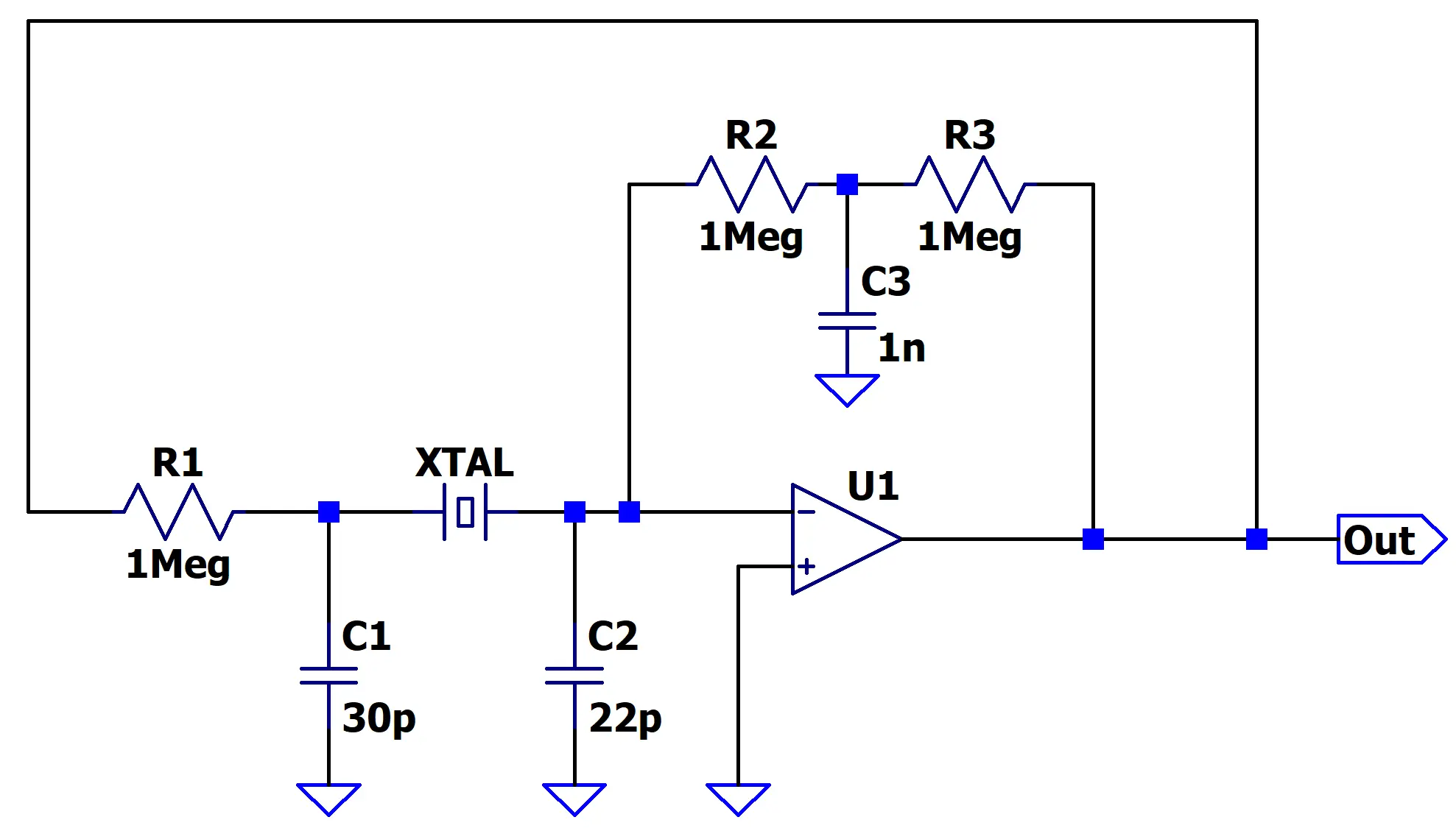
In this diagram, U1 represents our three transistor differential amplifier. At its core, the topology is a basic inverting amplifier, inverting — of course, because we need the 180 degree phase shift to make a Pierce Oscillator. As mentioned in the previous post.
You’ve probably noticed that the feedback network — R2, R3, and C3 — is a little unusual. I’ve set it up this way to work around a limitation in the crude three-transistor differential amplifier. You see, any feedback from the output to the inverting input is negative feedback that reduces gain. The discrete differential amplifier does not have much gain, and we can’t afford to waste a single drop of it. What I’ve done here is create a low-pass filter that blocks virtually all AC signals from reaching the inverting input, leaving the feedback network to set only the DC bias. In essence, with this feedback network, the differential amplifier operates at its full open-loop gain at AC frequencies.
With the high level view out of the way. This is the actual circuit as constructed:
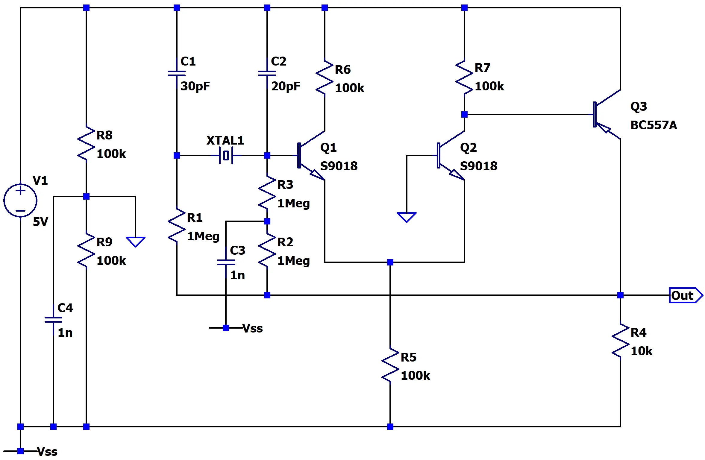
In this circuit, Q1, Q2, and Q3 form the differential amplifier represented in the block diagram by U1.
Q2’s base is the non-inverting input — as the output taken from its collector is inverted, then inverted a second time by Q3. This leaves Q1’s base as our inverting input.
R8 and R9 form a simple voltage divider that splits the rails evenly, with any noise shunted away by C3. The divider provides a virtual ground used to bias Q2, the non-inverting input.
Just as in the block diagram, R2, R3, and C3 form the feedback network that biases the entire amplifier.
Like the original circuit a trimmer capacitor is used for C1 so I can use it to fine-tune the oscillator’s frequency.
In contrast to our previous attempt this second attempt has a number of advantages:
- No need to fine-tune the bias point. It’s now managed by the feedback network and voltage divider, automatically adjusting based on the supply voltage.
- Very low input capacitance. Q1 acts as an emitter follower with a gain of approximately one, so there is no Miller effect—i.e., no amplification of the transistor’s junction capacitance by the gain.
- Extremely high input impedance. In the previous circuit, input impedance was relatively low. Here, it’s roughly β × R3, about 10 MΩ. This means the crystal isn’t heavily loaded, which should improve loop phase margin and startup time.
- Protection from parasitic coupling. Q2 acts as a common-base amplifier. Its grounded base electrically shields the input from the amplifier’s output, preventing loss of gain.
Overall, these improvements ought to make the oscillator more reliable, easier to set up, and faster to start.
Frequency Calibration
The previous version of the oscillator could not be calibrated to within specs, but thanks to the lower parasitic capacitances, it should now be possible, with any luck, to calibrate it to the correct frequency.
Let’s see where this one stands:
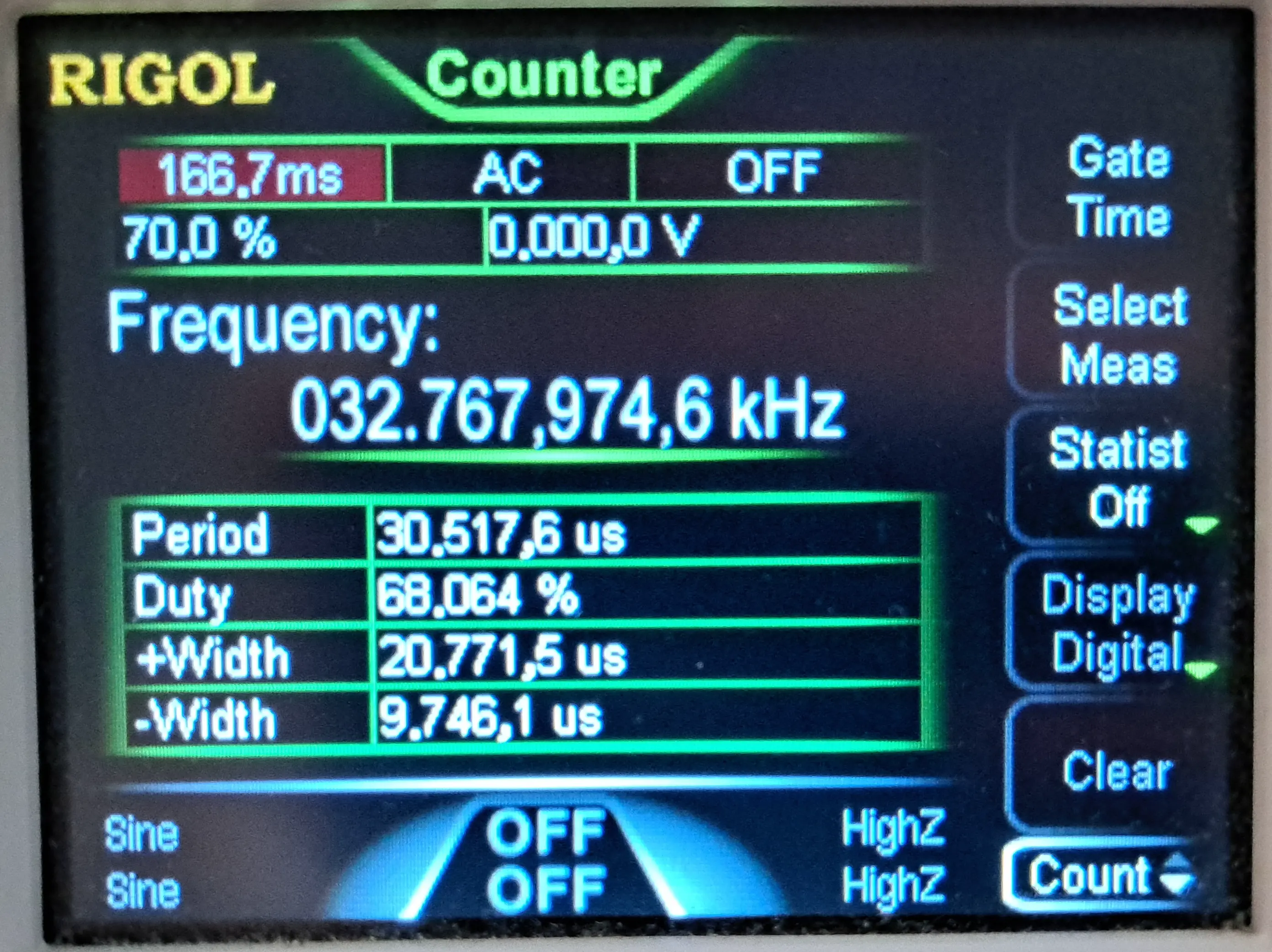
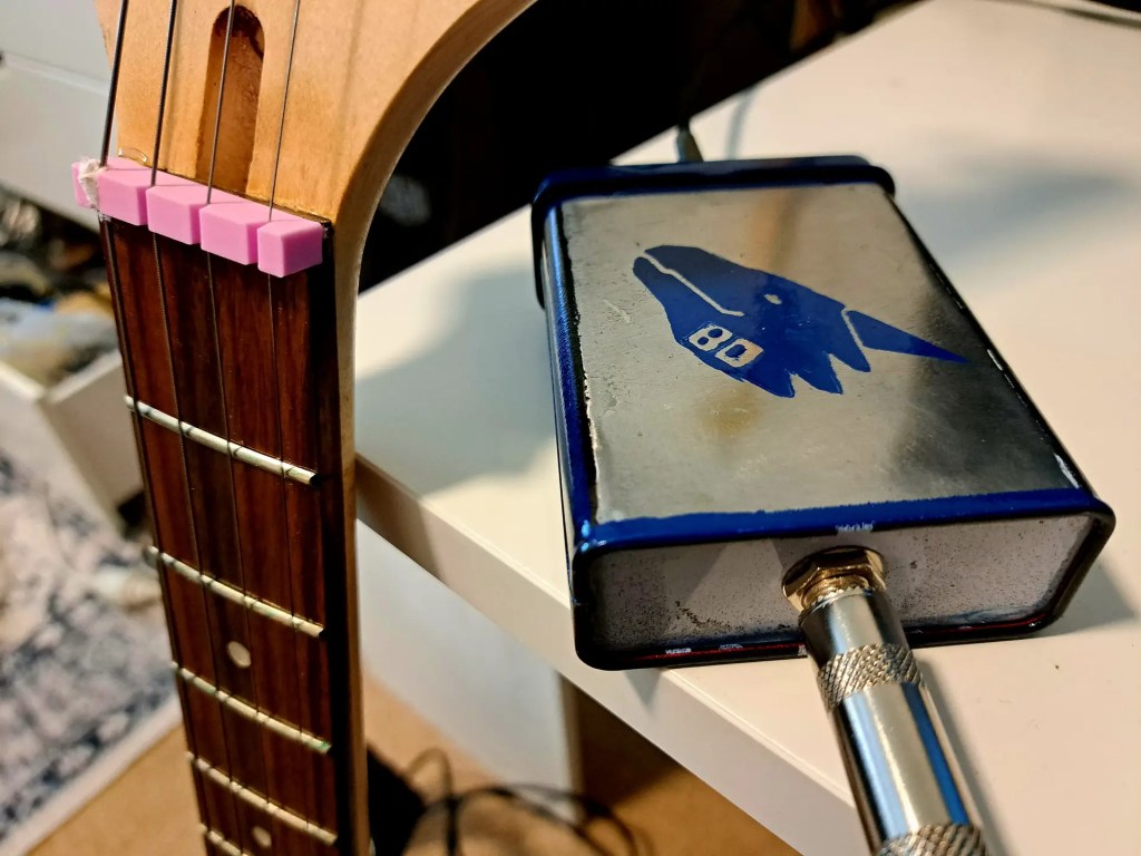
Hooray! Success at last. I was able to calibrate the oscillator to 32.767974 kHz
In parts per million error terms, that’s
Less than 1ppm error. Perfect! That’s well within the specifications of 20ppm. It won’t stay within that long term, but it demonstrates that I can successfully calibrate it.
Start Up time
The previous oscillator took almost eighteen seconds to start up. This one starts up in:
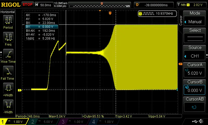
About 192 milliseconds after the power-supply stabilizes. Almost a 100X improvement.
Power Consumption
At 5V. The previous oscillator used 793μA. Now:
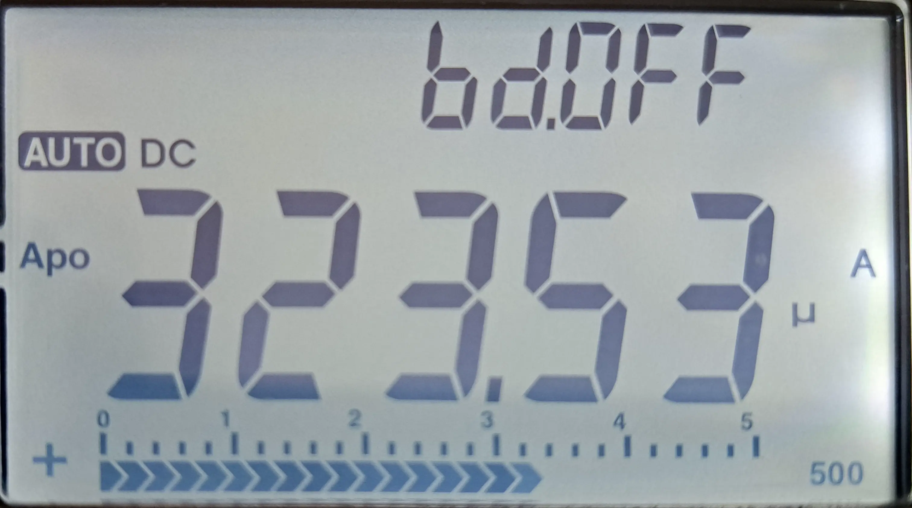
324μA. Less than 1/2 the current. The lower current is due to the fact this circuit is overall much higher impedance than the last.
At 3.3V the current reduces proportionally as expected:
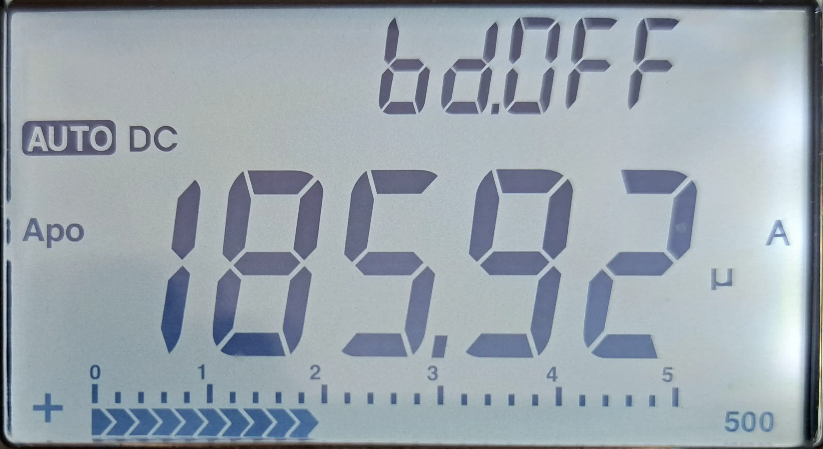
186μA. Not awful, but still an order of magnitude away what you could achieve with dedicated oscillator ICs. I didn’t spend any time trying to get this lower, it’d be interesting to see how low it could go. If anyone out there does better, drop me a line! But it only counts if it’s also the correct frequency!
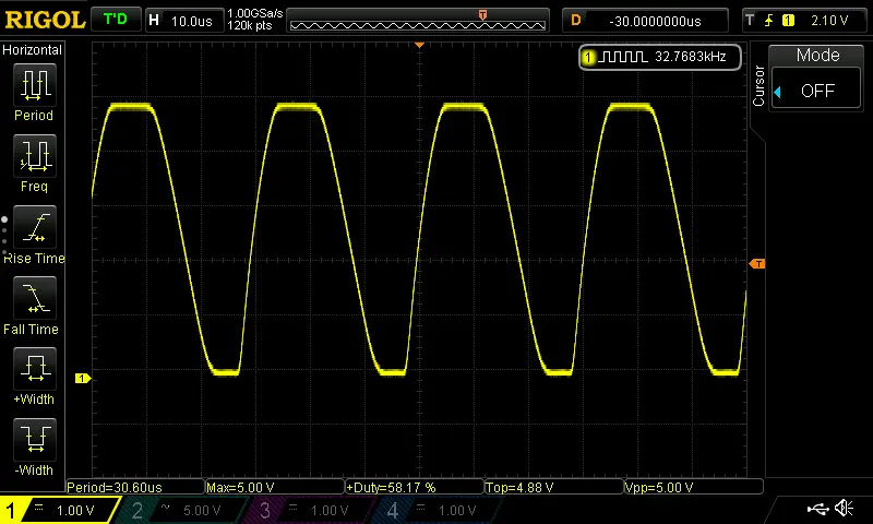
Waveform
For those interested, here is the oscillator waveform at 5V:
And at 3.3V:
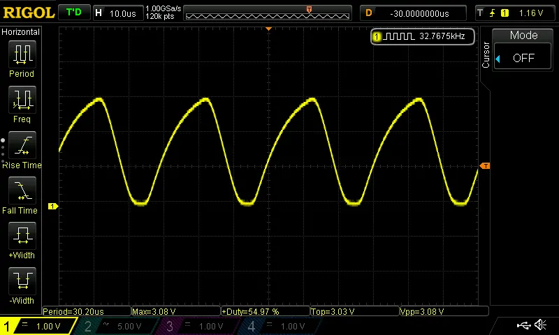
Not perfectly symmetric. But the edges are definitely clean enough, and the amplitude is high enough to trigger a digital circuit or micro-controller reliably.
The End
Finally, a summary of what was achieved with this circuit:
| Attempt 1 | Attempt 2 (this circuit) | |
| Oscillates at 5V | Yes | Yes |
| Oscillates at 3.3V | Yes | Yes |
| Current draw at 5V | 793μA | 324μA |
| Current Draw at 3.3V | 290μA | 186μA |
| Startup time | 18 seconds | 192 milliseconds |
| Frequency Accurate? | No (120ppm error, can’t be calibrated) | Yes < 1ppm error |
With this circuit I’ve managed to achieve all the original goals for the discrete low-frequency crystal oscillator. It runs at both 5 V and 3.3 V logic-level supplies without modification, and it can be calibrated to the specified frequency.
The complexity, however, has increased considerably. The design is now three transistors plus more than a dozen supporting components. That’s quite the contrast to the CMOS version, which uses only about half a dozen parts in total. It’s been an interesting learning exercise, but there’s no practical reason to use this discrete circuit in a finished product.
That said, there are still some avenues worth exploring if I feel like coming back to it. I could revisit the cascode variant, try to reduce the current draw, or experiment with JFETs instead of BJTs.
But for now, I’m done with this one. Time to move on to something else.

Leave a comment