
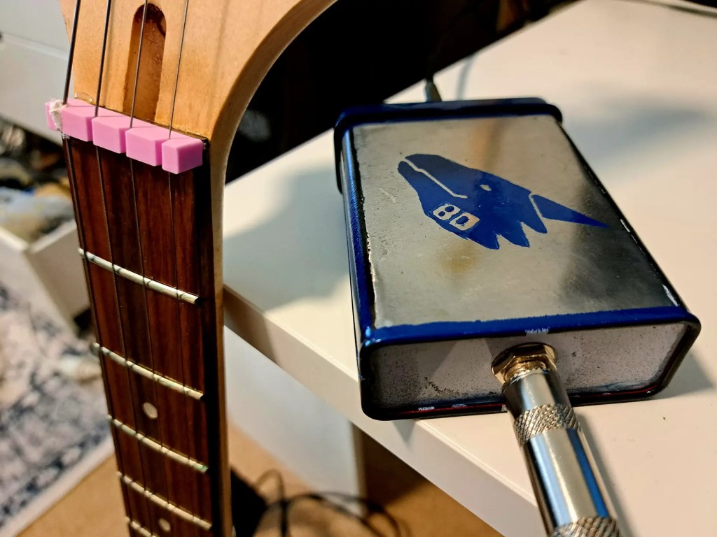
I’ll be honest from the start: when I began designing the SOT-223 LBA, my RF knowledge is far from complete. I wanted to build something educational—a flexible platform where I could learn by doing, make mistakes, and actually understand what was happening inside an RF amplifier rather than just copying cookbook circuits.
The goal was simple: see what kind of broadband linear performance I could squeeze out of cheap, off-the-shelf transistors. Could a basic 2N2222 and its complement give me clean amplification from 1 to 20 MHz? What would actually limit the performance? How much supporting circuitry would I need? I had no idea, but I wanted to find out.
I chose SOT-223 transistors specifically because they occupy a sweet spot for this kind of experimentation. It’s the smallest package that can handle around 1W while supporting proper thermal management through a tab that connects to a PCB thermal pad—smaller packages like SOT-89 don’t offer this capability. But beyond thermal considerations, SOT-223 offered several practical advantages:
- Low cost: Pennies per transistor instead of dollars
- Easier to drive: Smaller packages have lower input capacitance, making them more forgiving at RF frequencies
- Wide selection: Access to many high-frequency transistor options without needing expensive RF LDMOS parts or specialized amplifier modules
- Viable output power: 1-2W is modest, but it’s enough for a real transmitter—not just a laboratory curiosity
Anything larger felt like overkill for what I was trying to learn, and anything smaller wouldn’t give me the thermal headroom to experiment freely.

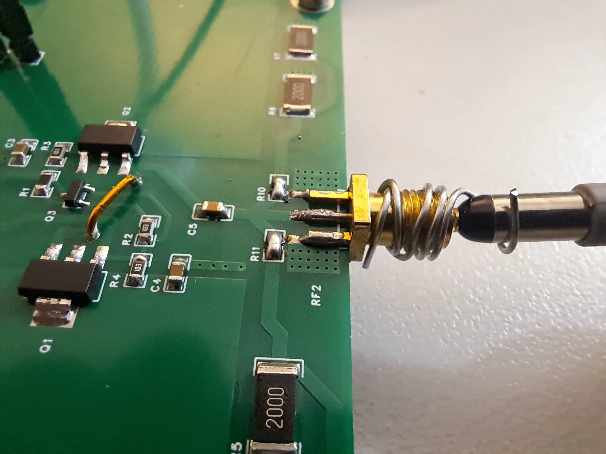
The circuit itself is straightforward: a class AB push-pull emitter follower using two SOT-223 transistors, biased with a Vbe multiplier. Nothing fancy, nothing proprietary—just the fundamentals.
Open Source
I’ve released this project under an open source license at OHSW Lab. You can download the PCB and the schematic there. You can also can get your own PCB at JLPCB for a mere $3.50! I’ll be updating the PCB with problems fixed, and new features as they are discovered.
Parts you’ll need
- 0805 Resistor Sample Book (AliExpress | Amazon)
- 0805 Capacitor Sample Book (AliExpress | Amazon)
- SOT-23 Transistor Sample Book (AliExpress | Amazon)
- Dupont/JST Connector Kit (AliExpress | Amazon)
- SMA Female Edge Connectors (AliExpress | Amazon)
- PZT2907A (LCSC)
- PZT2222A (LCSC)
Board Features
I’ve include a few features designed to maximize the module’s flexibility for experimentation.
Features such as
Input Matching Network
Footprints have been added to support a simple two-stage matching network at the input. The pads support 0805 capacitors and larger 1206 inductors rated for 0.5–1A, giving the flexibility to experiment with different impedance transformations.
The matching network consists of components labeled with “N” (for network):
- CN1: Parallel capacitor (0805)
- LN1: Parallel inductor (1206)
- CN2: Series capacitor (0805)
- LN2: Parallel inductor (1206)
For this initial testing, I bypassed the matching network entirely by bridging CN2 with a 0Ω resistor and leaving the other pads unpopulated.
Warning – The values given for the matching network are placeholder values. Calculate your own L matching network, or bypass by leaving all pads unpopulated and bridge CN2.
I wanted to characterize the raw performance of the transistors first before introducing any tuning—matching experiments would come later.
These network pads are small and should add negligible extra parasitics at the modest frequencies I intend to support.
On-board dummy load
I didn’t want to transmit my mistakes and experimental noise onto the air, so I needed a good dummy load. Commercial RF dummy loads can be expensive, and ensuring they present a clean 50Ω across a wide frequency range isn’t always straightforward. So I built one directly onto the module.
The dummy load uses four 200Ω resistors in parallel (2512 package)—the largest, highest-dissipation footprint I could find that’s still commonly available and cheap. At just 3 cents each and rated for 1W dissipation, all four in parallel give a generous 4W total capacity. This is probably overkill—I could have gotten away with two—but I was optimistic about the module’s capabilities.
Resistors in the 2512 package have parasitic inductance around 10nH and capacitance of just 1pF, giving a self-resonance near 500 MHz. Operating well below 20 MHz means I’m at less than 10% of this frequency, so the load should present nearly ideal 50Ω real impedance for measurements. To verify this performance, I measured the load with a VNA
The dummy load can be enabled by bridging pads R10 and R11
Generous Thermal Management
Using Understanding Thermal Characteristic of SOT-223 Package application note as a guide, I learned that SOT-223 can handle surprisingly high dissipation—if you give it enough copper.
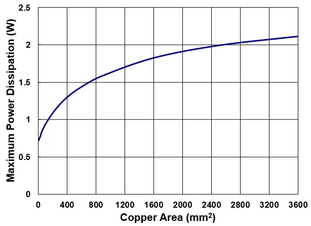
I added thermal pads to each transistor with a copper area of 1421 mm²—the maximum I could fit while staying within JLCPCB’s $3.50 prototype pricing tier. This provides thermal capacity for a little over 1.5W per transistor. With two such pads, the total board dissipation exceeds 3W, meaning with the right transistors, this design might eventually support 5–6W of RF output at 60% efficiency.
Testing
On-board dummy-load Validation
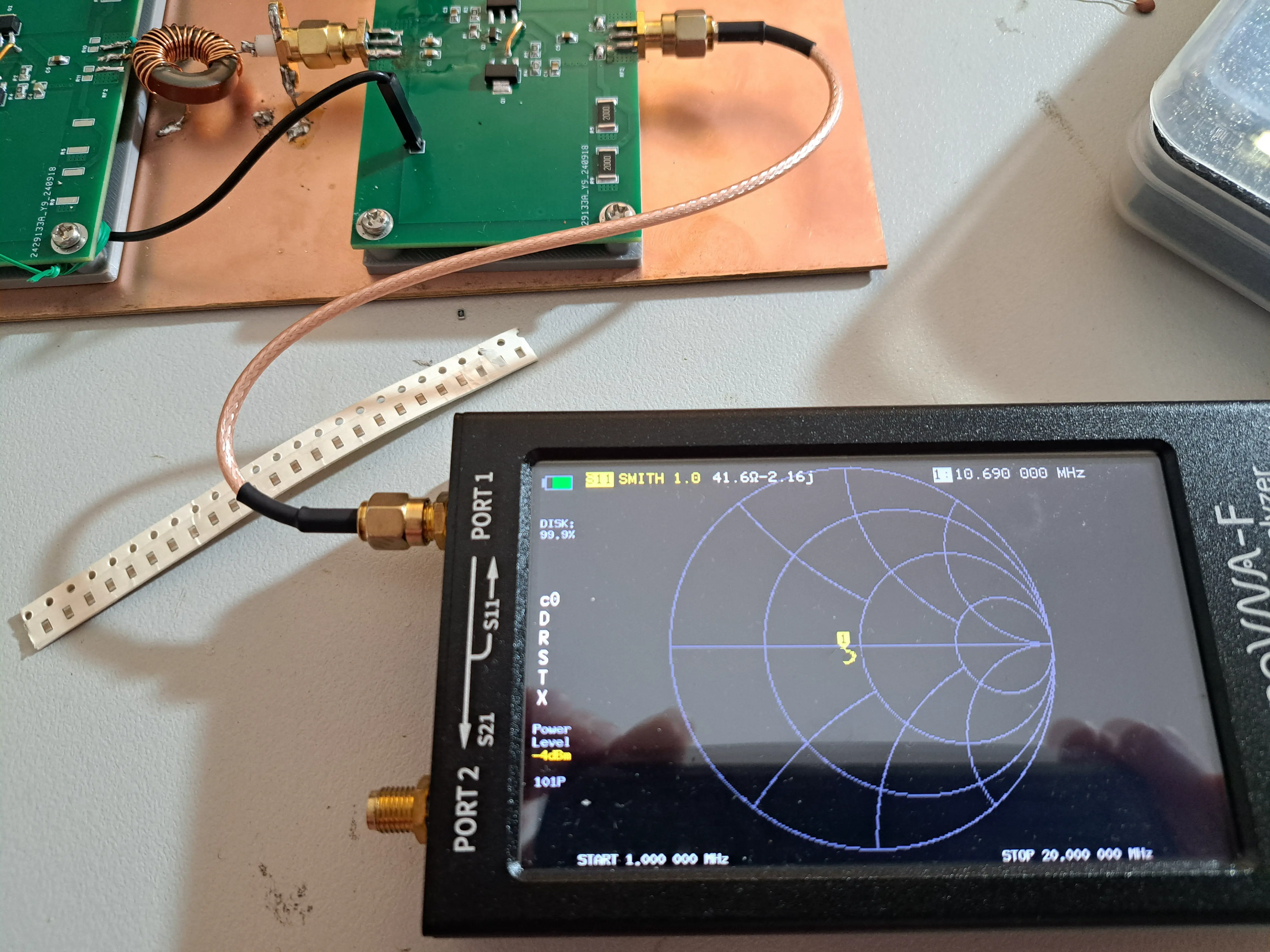
Before any further testing can commence. I make sure the on-board 50 ohm dummy load is performing as expected, to do this. I simply connect my NanoVNA to the output and scan from 0 to 20MHz the examined the resulting smith chart:
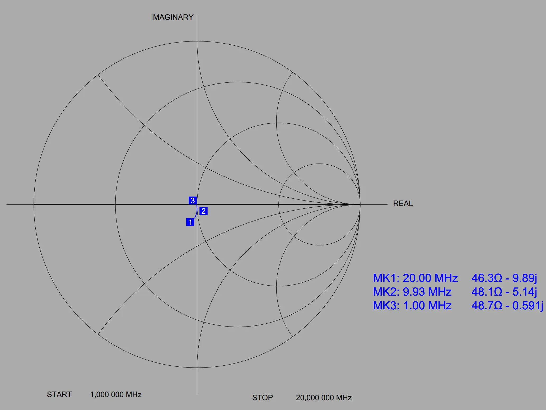
This result is more than acceptable. An ideal 50 Ω load would appear as a single dot at the center of the chart, but our trace deviates slightly downward, indicating a small amount of unwanted capacitive reactance of about –9.89 Ω.
To determine whether this is significant, we can convert this reactance into an equivalent capacitance:
About 35 pF — this matches what we expect from the transistor junctions and PCB parasitic capacitance at these frequencies.
The final measured impedance is close enough to a pure 50 Ω that, if we approximate it as 50 Ω, the measurement error is only around 10 %.
Maximum power into 50 Ohms
I intended to use my Rigol function generator to generate a test signal, above 10MHz my function generator can only produce a maximum amplitude of 10Vpp, however the module can handle a maximum of closer to 40Vpp.
To address this issue I constructed two of the modules and linked them together with a step-up auto-transformer wound on a T50-2 core. Relying on the 1:4 ratio to boost my 10Vpp into 40Vpp — enough to test the maximum output of the module.
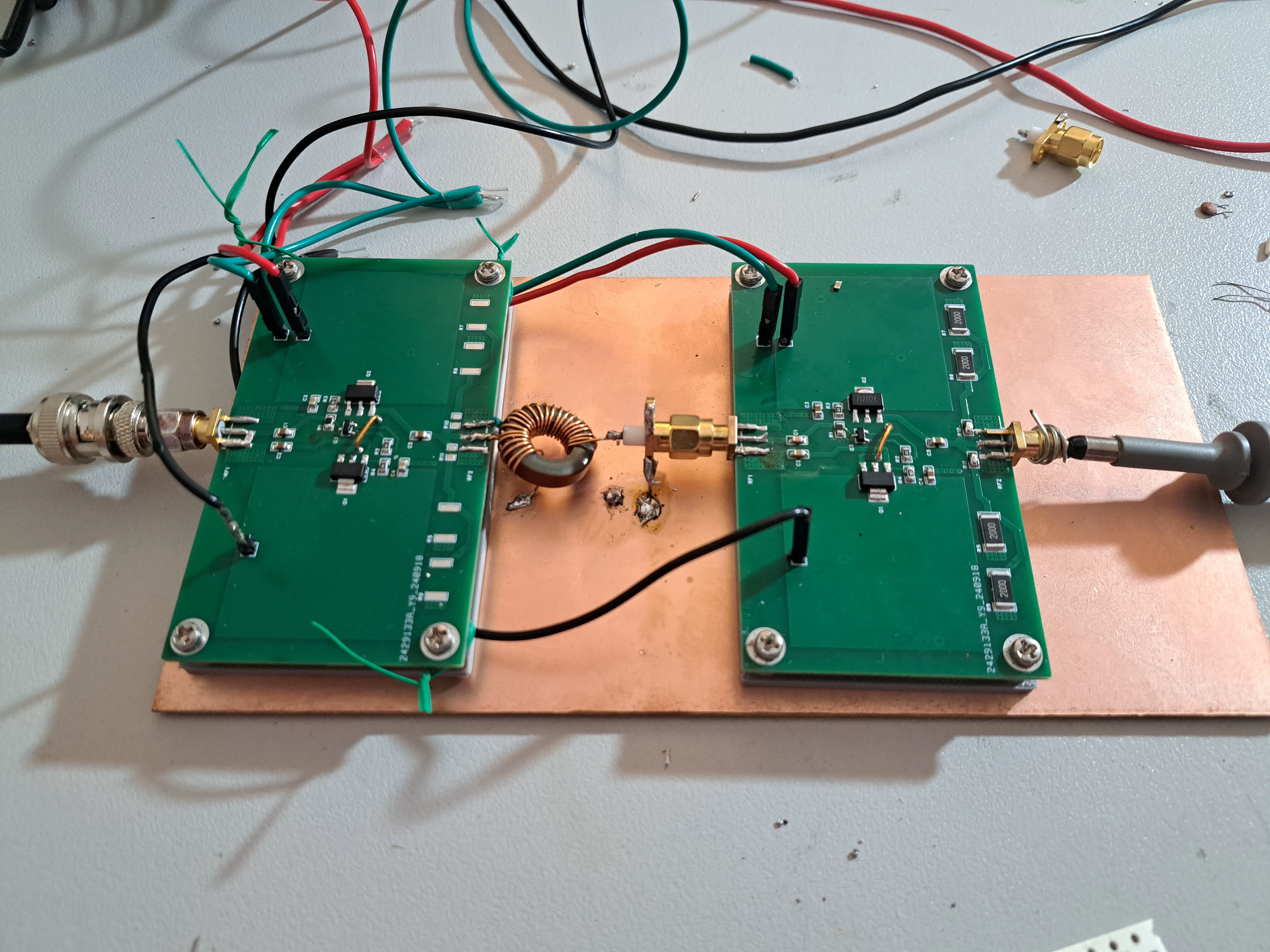
With two modules coupled together, I was able to test the maximum power output, during this test the module was run on +-17V so the theoretical maximum output would be just shy of 30Vpp
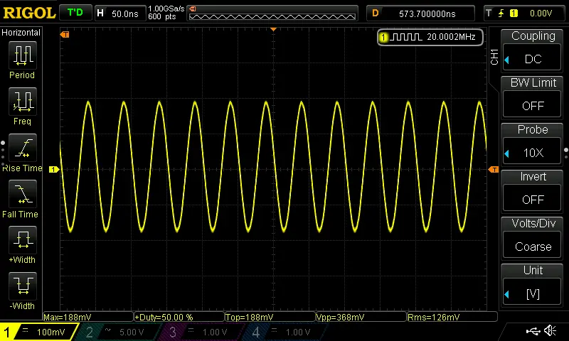
I probed the output with a standard 10X probe and recorded the waveform on my oscilloscope:
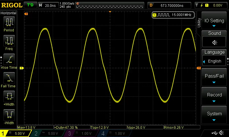
At 9.26 Vrms output, a small amount of crossover distortion is visible—an indication that the bias voltage isn’t quite high enough, allowing both transistors to turn off briefly during the zero crossing.
This is a known issue, as I omitted the emitter resistors, which help improve thermal stability. Too much bias current in this version of the buffer leads to thermal runaway.
However, for RF applications, this level of distortion is typically negligible and will be filtered by bandpass filtering or system resonances in practical use.
Now, to calculate the output power:
1.72 W—not too bad for generic transistors at 20 MHz. Though modest, this is enough power to transmit hundreds of kilometers on the HF bands using CW modulation (morse code) with a well-matched antenna.
Input Impedance
Finally I’ll examine input impedance. I connect the NanoVNA to the input of the HF-LBA to create another Smith chart.
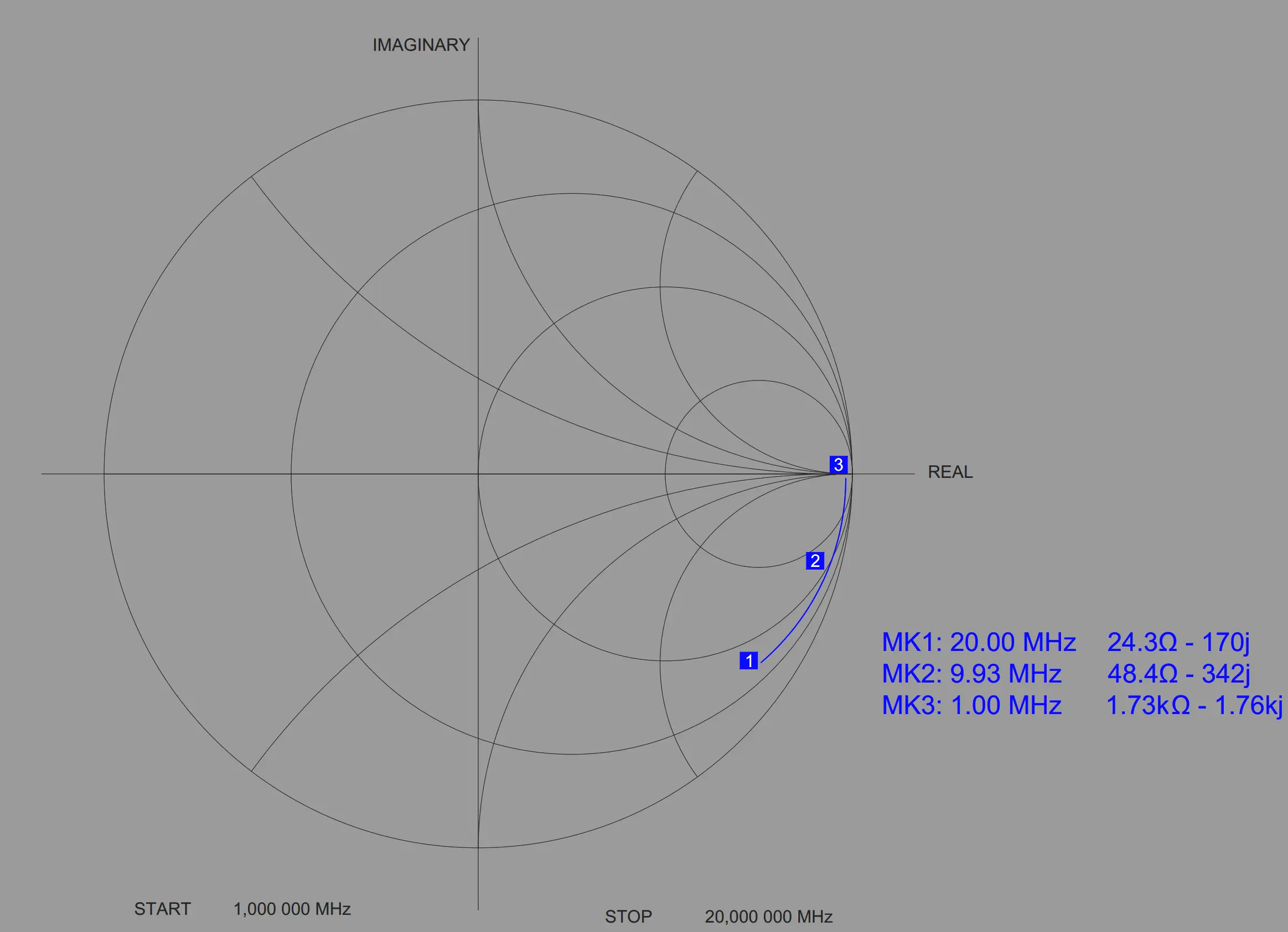
Looking at the input, I want the impedance to be as high as possible, since the amplifier’s current gain depends on the ratio of output to input impedance. Unfortunately, something seems off: the input impedance looks reasonable at 1 MHz but drops sharply at 10 MHz and 20 MHz.
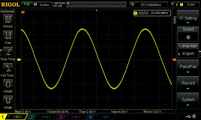
I suspect the NanoVNA is reporting correctly; the issue is likely that the impedance varies with input voltage. To sanity-check the VNA results, I probed across the input while injecting a 5 Vpp reference signal from my function generator.
This is the view across the input at 20MHz:
So, this is what we know at 20MHz:
- NanoVNA measured impedance = 24.3Ω – 170j
- Function generator source impedance: 50Ω
- Function generator output voltage: 5Vpp
- Observed buffer input voltage: 4.84V
Next we want to calculate |Z| from the NanoVNA, and from the function generator, to see if they are the same:
For the NanoVNA, the magnitude of the input impedance is:
For the function generator, we can calculate the input impedance using the voltage divider formed by the generator’s 50 Ω source and the buffer input:
The impedance measured with the function generator is much higher than what the NanoVNA reports and is actually very good, with 1512Ω input, and 50Ω output at 20MHz our gain is 30X, quite respectable.
Is the NanoVNA correct at all?
Being ever-curious, I decided to verify whether the NanoVNA’s reading makes sense. The NanoVNA is configured with an output power of -4 dBm. Knowing the 50 Ω load, we can convert this into the corresponding peak-to-peak voltage, which can then be applied using the function generator to double-check the NanoVNA’s result.
I round this value to 400mVpp and set the output of the function generator to match. Then I measure across the input to the buffer.
I get a result across the load of 368mVpp. across the load—just the same as before. I’ll now calculate the magnitude of the input impedance from this value to see if it matches the VNA result.
This close agreement shows the NanoVNA measurement is accurate for small‑signal conditions.
I repeated the tests at 10MHz and 1MHz, but there was virtually no measurable voltage drop, here’s the final table for the input:
| Frequency (MHz) | Vpp (V) | |Z| (Ω) |
| 1 | 5 | >10,000 |
| 10 | 4.96 | 4116 |
| 20 | 4.84 | 1500 |
Overall, this is a great result, the buffer covers the entire range of 1 to 20MHz comfortably without the impedance falling too low.
Final Specifications (With PZT2N2222A and PZT2907A transistors installed)
- Supply voltage: +17 0 -17V maximum +5 0 -5V minimum
- Peak RF output power 1.7W @ 20Mhz
- Frequency range 1MHz – 20MHz < 3dB
- Wide-band linear operation.
- Gain: 29.5db @ 20MHz
Known issues and next steps
Issues
- Add small (1 ohm?) emitter degeneracy resistors to improve thermal stability
- Test input L network matching
- Include footprints for an output matching network
- Create a rig that lets me measure IMD — intermodulation distortion for people interested in SSB usage.
Next Steps
Look forward to further VNA experiments, as well as experiments using input and output matching network, all using this very same module!

Leave a comment