
This tiny pre-amplifier converts the low-voltage, high-impedance signal from a guitar into a low-impedance, line-level output—making it suitable for direct connection to a sound card or other consumer audio equipment.
Guitar preamps aren’t complicated, but there’s plenty of ways to make mistakes. Get the virtual ground biasing wrong and you’ll introduce noise. Skimp on decoupling or use an improper ground layout, and you’ll get oscillation or hum. Miss the mark on input impedance and your tone suffers.
This project is about trying to avoid those pitfalls. I built a compact preamp that draws just 1.7mA at idle—roughly 30 continuous hours on a 9V alkaline battery—by carefully handling the design choices that many circuits gloss over. The result is a tiny, efficient circuit that sounds clean and behaves predictably
Features
The basic preamp circuit is straightforward, but the details matter enormously. This design has a no-frills focus on the fundamentals: proper virtual ground biasing, solid decoupling strategy, correct input impedance, and careful grounding to minimize noise and power consumption.
Many preamp designs online address these things haphazardly or not at all. This one treats them as the core of the design. The standout results are:
Low Power Draw — At just 1.7mA idle current, this preamp will run for roughly 30 hours on a standard 9V battery. That’s not just good for portability; it means there’s no chance of an unexpected mishap during a session.
Wide Operation Voltage — Functions perfectly at voltages as low as 3.3V, or as high as 16V. Giving plenty of power supply choices.
Modern Input Stage — We’re using a rail-to-rail CMOS input opamp, which means better signal handling, lower noise, and direct coupling options that older designs had to work around with coupling capacitors.
Reverse Voltage Protection — A P-channel MOSFET on the power line protects the circuit if you accidentally swap the battery polarity. No magic smoke, no ruined components.
Tiny Footprint — By committing to surface-mount components (SMT), the entire circuit fits on a board smaller than a business card. Perfect for effects pedals, portable rigs, or embedded in other gear. This small foot-print also means it fits into JLPCBs $3.50 pricing tier. You can get five boards for less than the cost of a coffee.
The Op-Amp
The selection of an op-amp is one of the few places in a guitar circuit where the choice truly matters. For decades, the TL072 has been the default—and it remains a solid device. With low noise, a 5.25 MHz bandwidth, and reliable performance, it has been in continuous use since 1978 for good reason.
However, that familiarity often persists long after the design constraints that made such parts popular have changed. Many modern audio circuits are single-supply, battery-powered, or expected to operate cleanly at 3.3 V. These are conditions the TL072 was never designed to optimize for, and its limitations—restricted output swing, higher current draw, and phase inversion under overdrive—become increasingly relevant in these contexts.
The COS9162 reflects a different set of design priorities. Manufactured by Cosine Nanoelectronics, it represents a newer class of low-power, single-supply op-amps developed for high-volume consumer and embedded applications. While companies like TI and Analog Devices dominate in the hobbyist and audio communities, smaller Asian manufacturers can offer good performance, viable alternatives, at rock-bottom prices if you’re willing to hunt through datasheets.
The COS9162’s rail-to-rail input and output stages allow full use of the supply voltage, translating directly into greater signal headroom on battery power. This also enables clean operation at 5 V—ideal for USB supplies, phone chargers, or other low-voltage sources. The TL072 simply isn’t well suited to this role; its limited output swing makes 5 V operation impractical for audio preamps.
The COS9162 also avoids phase inversion under overdrive, a known and unwelcome behavior of the TL072. It is unity-gain stable, operates from 3 V to 16 V, and costs approximately $0.28 per chip. As an additional benefit, it is significantly quieter, with a noise density of 10 nV/√Hz compared to the TL072’s 37 nV/√Hz at 1 kHz.
The TL072 remains a well-understood and familiar part in the DIY and guitar electronics community. But with lower power consumption in dual-op-amp designs, true 5 V compatibility, immunity to phase inversion on overload, lower noise, and a rock-bottom price, the COS9162 is well worth consideration.
Parts you’ll need
- 0805 Resistor Sample Book (AliExpress | Amazon)
- 0805 Capacitor Sample Book (AliExpress | Amazon)
- SOT-23 Transistor Sample Book (AliExpress | Amazon)
- COS9162 Op-Amp (LCSC)
- Dupont/JST Connector Kit (AliExpress | Amazon)
- Effect Pedal Enclosure (AliExpress | Amazon) (For the classic look)
- Mini Toggle Switch (AliExpress | Amazon) On-Off Switch
- 6.5mm Panel Mount Jack (AliExpress | Amazon)
- 3.5mm Panel Mount Jack (AliExpress | Amazon)
- The PCB (Gerber file)
- You can also get. The EasyEDA source files Consider them BSD licensed.
Schematic

The schematic is relatively simple, but care has been taken in several areas:
Virtual Ground
The virtual ground and biasing network for single-supply operation has been has been taken from recommendations given in these analogue devices application notes, a configuration has been calculated from these notes that maintains good power supply noise rejection ratio (PSRR). Something easily compromised when creating single-supply amplifiers.
The virtual ground splits the 9 V supply into a bipolar ±4.5 V system, creating +4.5 V, 0 V, and -4.5 V rails. Capacitor C2 is critical, as it stabilizes the virtual ground against power supply noise; without it, the high supply rejection normally provided by the op-amp is severely degraded. Circuits that rely solely on a resistor divider should be avoided.
RF Noise Rejection
The feedback loop and input path include components to reject RF noise. As frequency approaches 100 kHz, C6 and C7 present a low impedance. C6 shunts RF noise on the input to ground, while C7 allows high-frequency noise to bypass the feedback voltage divider, preventing RF interference from being amplified.
High Input Impedance
I chose an non-inverting configuration so we can have simple control over the input-impedance of the amplifiers. Here R3 sets the input to a guitar standard of 1Mohm. If you’re environment is noisy, you can reduce this value, but reducing it too far may impact your tone.
Gain
R5 and R6 set the gain according to the formula:
Here, the gain is set to five. A gain adjustment potentiometer is intentionally omitted; once set correctly, there is little need to change it. Long wires and a potentiometer in the feedback path can have a detrimental impact on noise performance. Instead, overall level can be controlled using the guitar’s volume knob, keeping the circuit simple and minimizing confounding variables.
Capacitive Loads and Stability.
R9 and R4 are series (or isolation) resistors. They prevent the op-amp from oscillating when driving highly capacitive loads, such as the PCB ground plane in the virtual ground circuit or the shielding on an audio cable. They do this by adding a small series impedance between the op-amp output and the capacitive load, which reduces the phase shift at high frequencies and prevents the feedback loop from becoming unstable. While some circuits omit these resistors, including them here improves stability and overall robustness.
While some circuits omit these resistors, including them here improves stability and overall robustness.
Input Protection
A P-channel MOSFET provides reverse-voltage protection by being placed in series with the positive supply rail, with its source connected to the battery and drain to the circuit. When the battery is installed correctly, the MOSFET turns on automatically due to the voltage difference between source and gate, allowing current to flow with very low on-resistance. If the battery is inserted backwards, the MOSFET stays off, blocking current and protecting the circuit. Compared to a diode, this method has a significant advantage: it introduces almost no forward voltage drop, leaving more of the battery’s voltage available for the amplifier and improving overall efficiency.
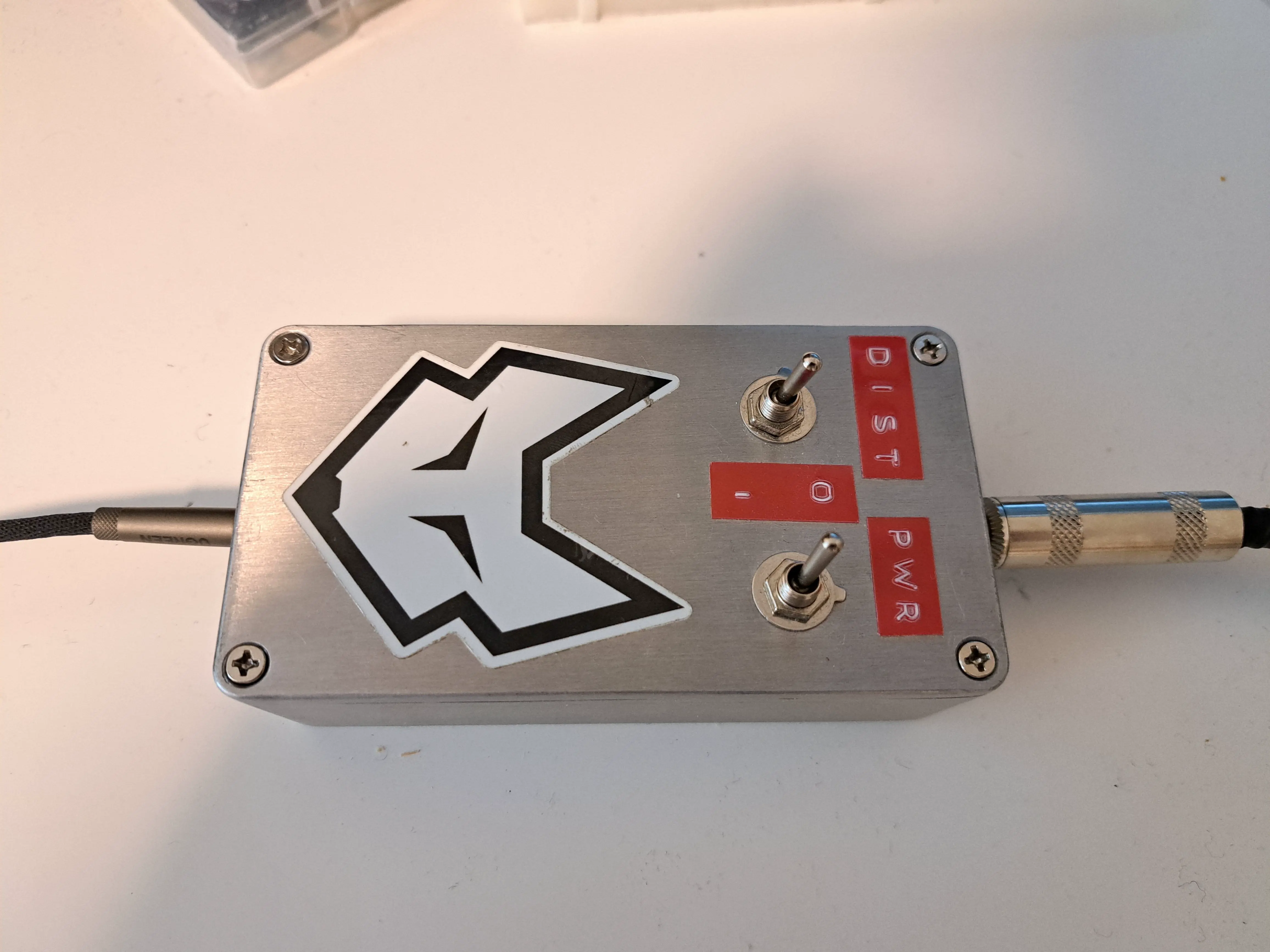
Case
Whatever enclosure you choose, metal is best for lowest noise. Connect it to GND (the analog 0 V) shown in the schematic—not PGND, which carries power currents. Tying the shield to GND provides a low-impedance path for interference currents and helps reduce hum and RF pickup in the circuit.
Result
One of the most important parts of the build is the battery consumption, so first thing after building the circuit I measure the current:
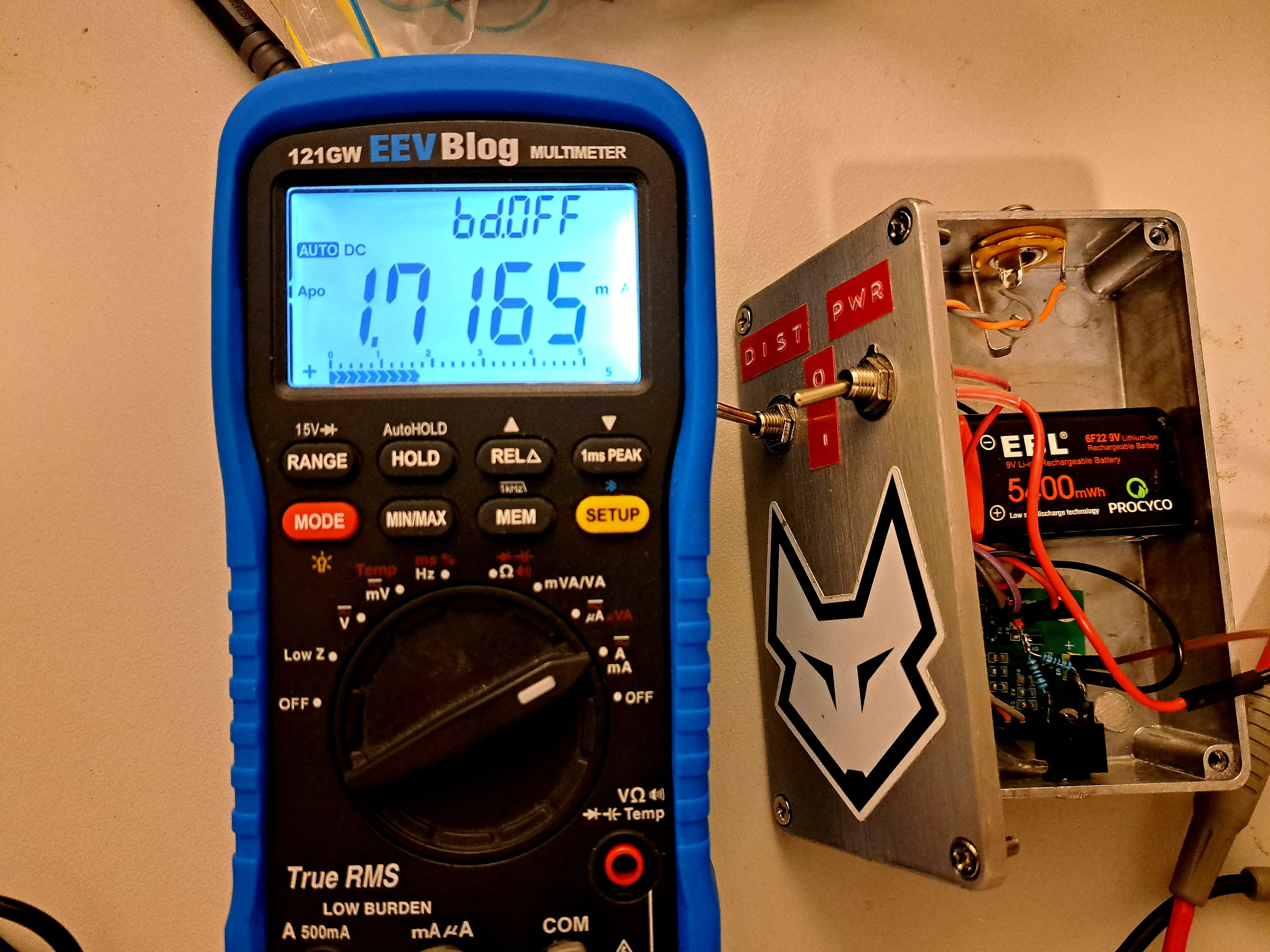
1.72mA — Looks good. Very close to the datasheet’s claimed 0.9mA per amplifier. The virtual ground’s resistor divider network should only constitute around 0.020mA of this, basically negligible. A 9V battery should last many months intermittent playing at this power draw.
I checked the circuit for oscillations on my oscilloscope, both with and without cables plugged in. Everything looks fine, dead flat output.
I haven’t measured the noise or frequency response, but first impressions are good. Perhaps the proof of the pudding is in the eating though, so here’s a few samples taken from the pre-amp. I’m only a beginner at guitar, with only 12 months experience (at time of writing) you’ll have to excuse my clumsy playing:

Leave a reply to A Battery-Free Guitar Input for Your Sound-card – Silicon Junction Cancel reply