
In my previous post I discussed my build of the slayer exciter Tesla coil and provided a few tips to make the circuit a little more robust. This post is a follow-up with a more advanced and much more powerful version of the slayer exciter.
This updated design addresses a couple of key shortcomings of the original circuit:
- When higher-current transistors (such as the 2N3055 and its variants) are used, a single gain stage does not provide sufficient current gain for clean, reliable switching.
- The transistor in a basic Slayer Exciter dissipates more heat than necessary because it spends a significant amount of time operating in the active region rather than fully saturating.
These issues can be mitigated by updating the circuit to use a MOSFET instead of a BJT and, most importantly, by introducing a dedicated MOSFET gate driver. The driver enables much faster transitions between the off state and full conduction, minimizing the time spent in the linear region. These upgrades allows substantially more power to be delivered to the coil along with significantly reduced device heating.
Parts you’ll need
- Magnet wire (0.5mm) (AliExpress | Amazon)
- 1N5819 Schottky Diode (AliExpress | Amazon)
- Assorted Resistors (AliExpress | Amazon)
- Assorted Electrolytic Capacitors (AliExpress | Amazon)
- IRF540N (LCSC)
- TC4429 (LCSC)
- LM7809 (LCSC)
Schematic
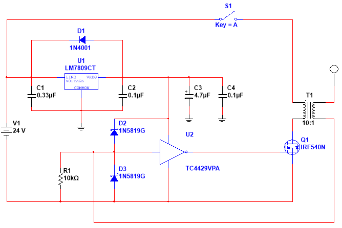
As in the previous post, D2 and D3 must be Schottky diodes; standard diodes are not fast enough and may allow high-voltage transients to damage U2. It is also critical that D2, D3, C3, and C4 are placed as physically close to U2 as possible. Do not omit these capacitors—without them, the driver will run very hot.
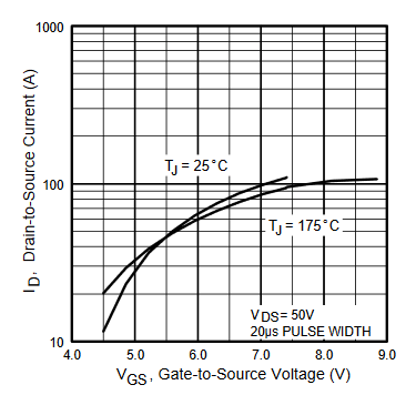
U1 supplies 9 V to power the gate driver and may require a small heat sink. A 9 V supply is chosen because Q1 is fully enhanced at a gate-to-source voltage of approximately 9 V. Driving the gate at a higher voltage reduces switching speed and increases power dissipation in the MOSFET driver. Conversely, driving the gate at a lower voltage increases the MOSFET’s on-resistance, shifting the dissipation to the MOSFET itself.
Q1 requires a decent heat-sink, don’t go too small. An old CPU heat-sink can work well here.
When selecting Q1 the main attributes to look for in the datasheet are:
1. Low Rds(on) resistance.
2. A maximum drain-to-source voltage (Vdss) of about 3 to 4 times the supply voltage
The IRF540n satisfies both of these criteria nicely:
- Rds(on): 0.044 ohm
- Vdss: 100V
If you don’t have a suitable MOSFET you can probably salvage a suitable one from an old PC (or other) switching power supply.
When selecting U2 the main attributes to look for are:
- Switching speed, ideally 40ns or lower
- High current, ideally 3A or more.
I’ve found in practice it’s possible to run MOSFET drivers in parallel, this helps them switch faster and run cooler. To do this you simply need to tie their outputs and inputs together. However ensure that each driver chip gets its own set of 0.1uF and 4.7uF capacitors. Scaling up the circuit to a much more powerful version should be possible by utilizing parallel MOSFETS and gate drivers together.
An important thing to keep in mind with this circuit is it will only operate if the current is passing through the primary in the right direction, if your circuit fails to oscillate, first try reversing the connections on the primary winding.
Completed
In my circuit I used two MOSFET drivers in parallel as I only had 1.5A drivers available and they ran hot with only a single driver:

Videos of this circuit in action:


Leave a Reply