
A capacitor, at its core, is just two conducting plates separated by an insulating layer. Charge accumulates on the plates, an electric field spans the gap, and energy is stored. It’s one of the most fundamental structures in electronics — and it turns out that structure exists naturally inside every diode.
When a diode is reverse biased, a region forms at the p-n junction called the depletion region. Free charge carriers — electrons on the n-side, holes on the p-side — are pushed away from the junction, leaving behind a zone that is swept clean of mobile charges. This makes it a poor conductor, much like the dielectric in a capacitor. On either side, the bulk doped semiconductor remains conductive, acting like the plates. Two conductive regions, separated by an insulating layer: it’s a capacitor, built right into the junction.
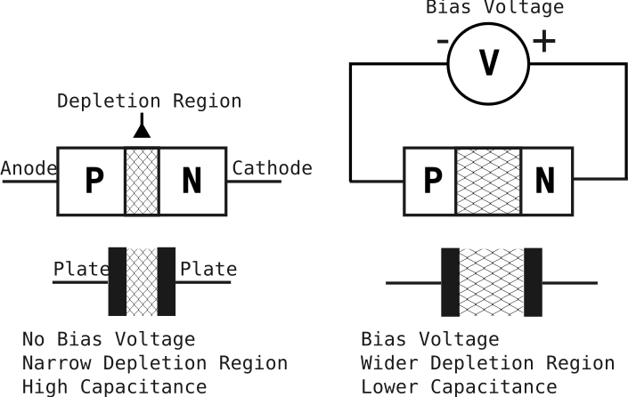
What makes this interesting is that the depletion region doesn’t have a fixed width. Increase the reverse voltage, and it widens — effectively pulling the plates further apart and reducing the capacitance. Decrease the voltage, and it narrows, increasing the capacitance. The relationship follows a curve determined by the doping profile of the junction, but the core idea is simple: you have a capacitance that you can control just by adjusting a DC voltage.
The Varactor
A component whose capacitance you can tune with a voltage is a useful thing — useful enough that a whole class of diode was developed around the idea. They’re called varactors, short for variable reactor, and they’re a staple of RF circuits, voltage-controlled oscillators, and tunable filters. But dedicated varactors are simply diodes optimized and characterized for this effect — every p-n junction diode already has it.
Every Other Diode
So if every p-n junction is hiding a varactor, the natural question is: how usable are they in practice? Dedicated varactors are characterized with precise capacitance-voltage curves and tight tolerances — but a bag of 1N4148s or a strip of LEDs pulled from a drawer? Not so much. To find out, I put a handful of common, everyday components into a test harness and measured how their junction capacitance varies with reverse voltage. The results might change what you reach for next time you need a tunable capacitor.
What You’ll Need
Test Harness
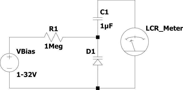
The test harness mirrors the topology a varactor would typically see in a real circuit. C1 is a DC blocking capacitor, isolating the bias voltage from the rest of the circuit. Because C1 appears in series with the varactor D1, it needs to be significantly larger in value — otherwise it will dominate the series combination and compress the effective tuning range.
The bias voltage is applied to the varactor through R1, which must be a high value to prevent it from loading the junction and disturbing the capacitance measurement.
To get a representative picture of what’s out there in a typical parts bin, I tested a range of common components: standard silicon rectifier diodes, fast signal diodes, Schottky diodes, LEDs, and BJT transistors — using the base-collector junction. I also threw in a selection of MOSFETs, using the body diode that exists inherently in every device.
To use an N-channel MOSFET’s body diode as a varactor, connect the gate and source together and treat this as the anode. The drain serves as the cathode.
A P-channel do the same thing, but the drain is the anode and the source is the cathode..
Here is a table of the results:
| Device | @ 1V (pF) | @ Vmax (pF) | Vmax (V) | Tuning Ratio |
|---|---|---|---|---|
| 1SV149 | 440.9 | 22.17 | 9 | 19.89 |
| IRFP460 | 5842 | 448 | 30 | 13.04 |
| NCE65T540F | 2912 | 238.6 | 30 | 12.20 |
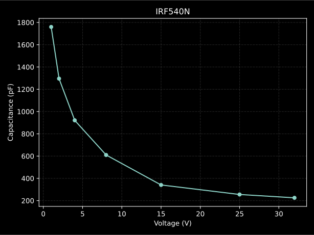
| IRF540N | 1759.8 | 225.2 | 32 | 7.81 |
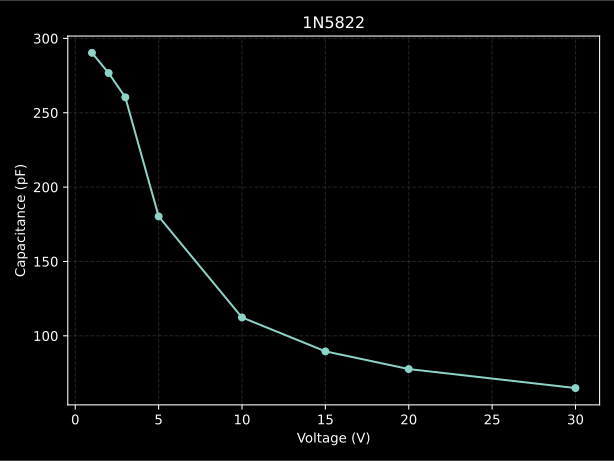
| 1N5822 | 290.3 | 64.84 | 30 | 4.48 |
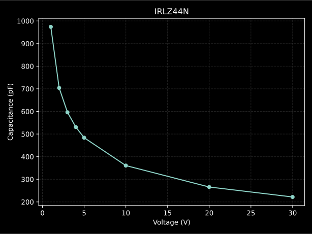
| IRLZ44N | 974 | 221.8 | 30 | 4.39 |
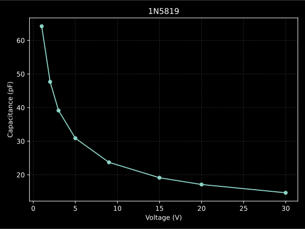
| 1N5819 | 64.22 | 14.65 | 30 | 4.38 |
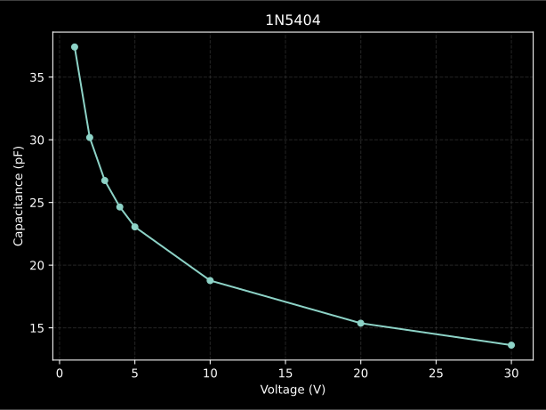
| 1N5404 | 37.4 | 13.62 | 30 | 2.75 |
| 2N7000 | 13.76 | 5.57 | 32 | 2.47 |
| 1N5711 | 11 | 4.58 | 32 | 2.40 |
| TIP31C | 289 | 187.4 | 5 | 1.54 |
| Blue LED | 21 | 14.5 | 5 | 1.45 |
| 1N4148 | 4 | 3 | 32 | 1.33 |
| Red LED | 6.28 | 5.55 | 5 | 1.13 |
Each device is characterized by its junction capacitance at 1 V reverse bias and at its maximum safe reverse voltage — which varies by device, as pushing all of them to the same voltage would exceed the ratings of some.
The best performer in the lineup is the 1SV149 which is a dedicated varactor diode intended for AM tuning — no surprises there. The rest of the devices follow a clear trend from best to worst:
- High voltage MOSFETs
- Low voltage MOSFETs
- High current Schottky rectifier diodes
- Silicon Rectifiers
- Everything else
The performance of the power MOSFETs comes down to physical scale and doping chemistry. Their massive junction areas provide a much higher baseline capacitance, while the lower doping concentrations required for high-voltage ratings allow the depletion region to expand more significantly under bias, yielding a larger tuning range.
Schottky rectifiers benefit from large junction areas that provide a high baseline capacitance. More importantly, their lower internal “barrier” (built-in potential) makes them more responsive; because the starting internal voltage is so low, every volt you apply from the outside has a much larger proportional impact on stretching the depletion region.

C-V Charts
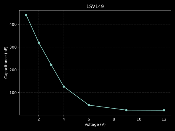
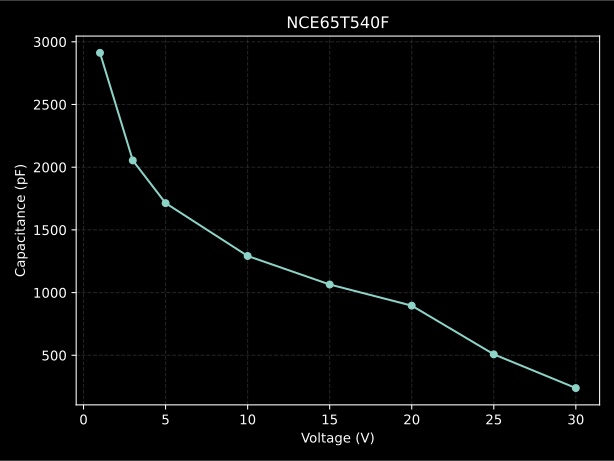
For some of the higher performing devices I’ve created capacitance vs voltage charts:
A note on applications
Dedicated varactors give you a well‑characterized C-V curve, tight tolerances, and often a wide tuning ratio.
But if your application doesn’t require that full range—say, a narrow‑band oscillator or a simple tunable filter—a common MOSFET or rectifier can work just as well.
The high reverse voltage ratings of power MOSFETs also make them a convenient fit for vacuum tube circuits, where a 100 V+ bias would exceed the ratings of most AM‑band varactors.
It’s not a replacement for precision parts, but it’s a useful option when you’re prototyping from the drawer.


Leave a Reply